Scalable techniques to produce graphene and new practical applications, an interview with INL Group Leader, Pedro Alpuim
May 31, 2021
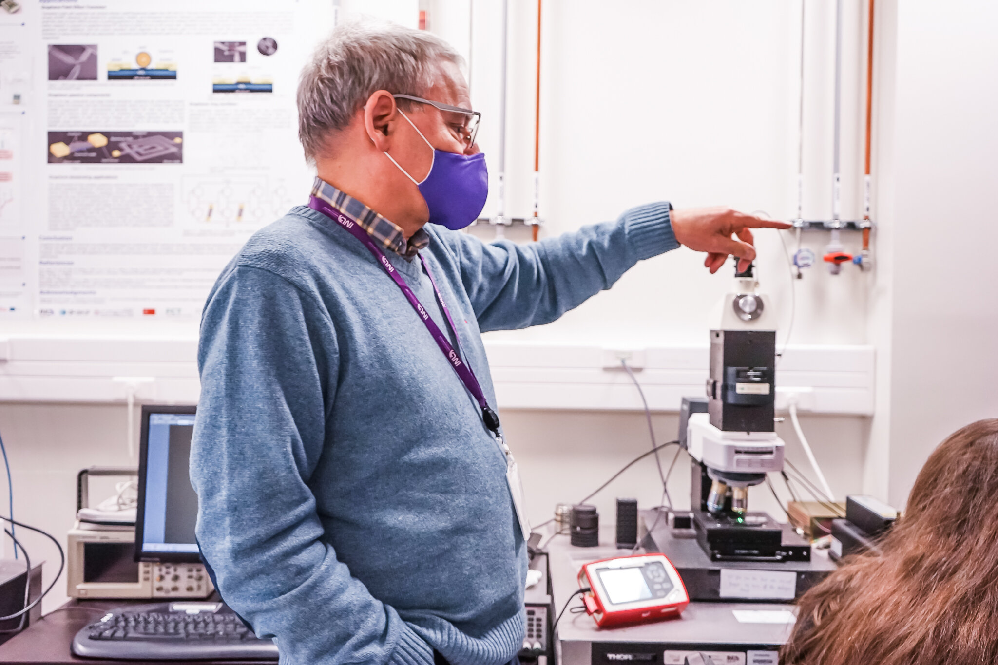
Pedro Alpuim is the 2D Materials and Devices Group Leader at INL. He works in CVD and 2D materials device fabrication, with an emphasis on biosensors. In particular, he develops graphene devices to detect biomarkers for medicine and environmental monitoring.
He received a PhD degree in Materials Engineering from IST Lisbon in 2003, working in amorphous silicon thin-film devices for flexible electronics, and an MSc in Physics from the UM and has published more than 90 papers in peer-reviewed journals and has h-index=24.
Can you tell us about your professional journey before arriving at INL, and what were the most important projects you’ve worked on?
I arrived at INL coming from the University of Minho, where I was (and still am) a professor in the Physics Department and before coming to INL, I installed a thin-film solar cell and semiconductor research lab at the University of Minho, in Guimarães.
Interestingly, that lab – including high-vacuum deposition systems for CVD, e-beam and thermal evaporation, and a semiconductor optoelectronic characterisation facility – was built with research equipment ceded by EU institutions based on trust and friendship at zero cost. I started to build that international scientific network during my PhD years working in flexible electronics at INESC-MN and IST, Lisbon, in Prof. João Pedro Conde’s group.
Before that, I worked as an MSc student in the KFA Jülich, Germany, in thin films’ mechanical properties, my first international experience as a scientist. Earlier, I was a secondary school teacher of physics and chemistry, which taught me how to communicate science to young people. Even earlier, I worked in a family-owned estate in wine production – Vinho Verde – helping to convert a centuries-old technology into a modern one. It was fascinating and, being then a physics student, opened my mind to the incredible richness of chemistry and biochemistry.
How did 2D Materials and Devices group start, and how does the group correlates with INL’s Research Strategy?
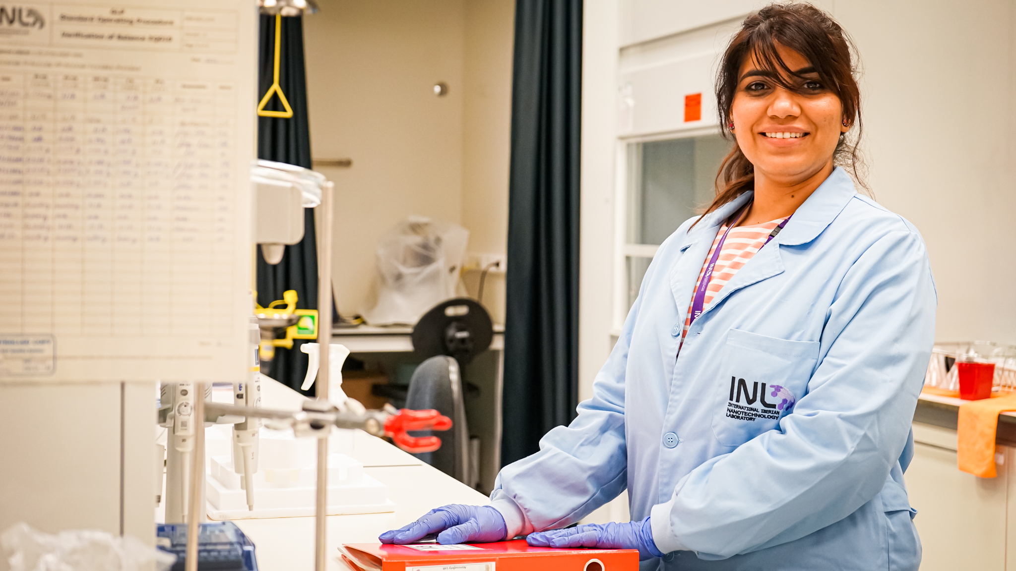
I arrived at INL in 2011 as a researcher from the Department of Physics of the UMinho to start applied research in graphene. Graphene was a new 2D material discovered some years before by Geim and Novoselov in 2004. In 2011, much of the incredible physics of graphene had already been elucidated, but graphene was known mainly by physicists and produced in a purely artisanal way in university labs by PhD students and post-docs using scotch tape. So the idea at INL was to develop scalable techniques to produce graphene and find a few practical applications based on its unique properties.
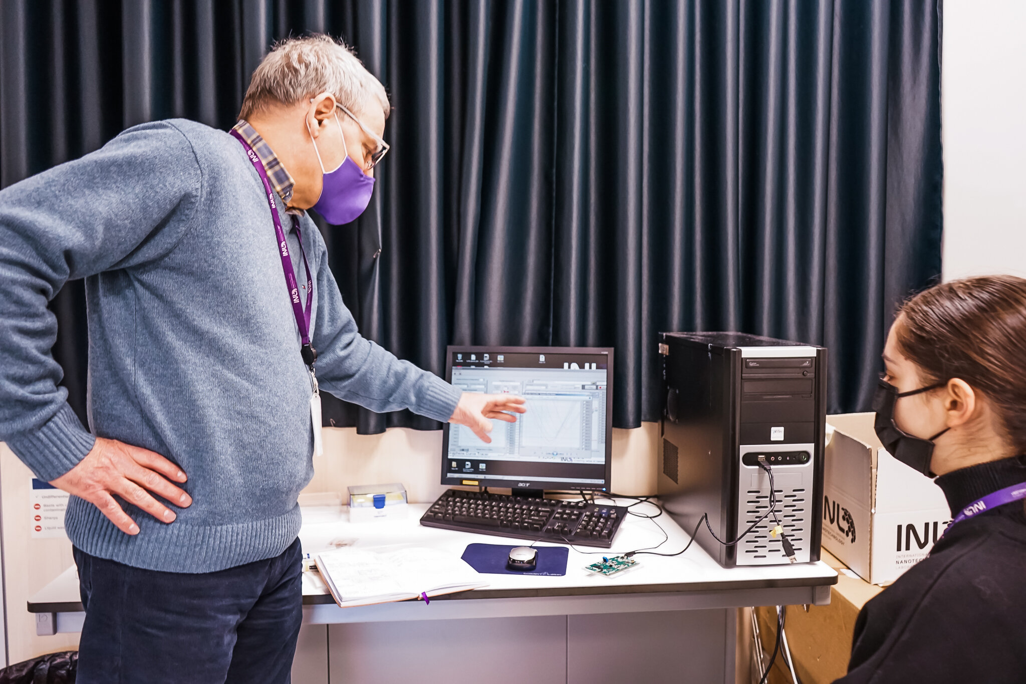
The first task I had at INL was to launch international tenders to purchase equipment to produce graphene. I then met Jérôme Borme, whom INL had hired before the Braga campus was finished, and was sent to Germany for an internship on graphene growth on metallic surfaces. We started the 2D materials and devices group that I first called the ‘Thin Film Devices Group’ since both Jérôme and I were in thin-film devices, magnetic devices, in his case, and in semiconductor devices. A few years later, when the laboratory was already equipped for graphene growth by CVD, and we had developed the first clean-room processed graphene wafers, the group’s name changed to 2D Materials and Devices. By then, we were also growing h-BN and planning to start working in transition-metal di-chalcogenides (MoS2 and 2MoSe2).
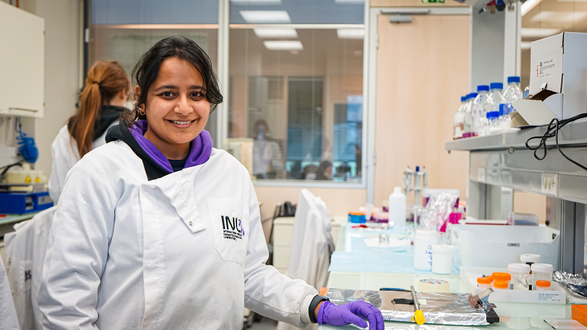
In 2015, we received a visitor from the Universidade Federal de São Paulo, Brazil – Nirton Vieira – who came with the idea of using our graphene in bio applications. Together, we developed the first electrolyte gate graphene transistors, which successfully detected biomolecules in solution. That strategy was particularly well aligned with the INL program in biomedicine. Motivated by these preliminary results, we started to work with Elisabete Fernandes from the INL Nanodevices group to functionalize graphene surfaces for immunoassays.
Shortly after, an electrochemist with a background in DNA sensors – Rui Campos – was hired to help develop the first graphene nanosensors. With those, we obtained a record limit of detection in the attomolar range of a 25-mer DNA sequence. We are now engaged in several projects developed around our graphene FET biosensors, from detecting counterfeiting in Port wines to Malaria or ischemic stroke early detection and neural interfaces for neurotransmission probing.
Meanwhile, the group has grown, and we now have Andrea Capasso coordinating the effort on the growth of hBN and MoSe2 for photonic and optoelectronic applications, including quantum computing technologies. Graphene conductive inks based on liquid-phase exfoliation of graphite for application in Li-ion batteries, electromagnetic interference shielding, and touch screen displays result from collaborative projects, also lead by Andrea. Two post-docs – Alexandre Chícharo and Juan Luis Pomar, this one with an individual Marie Curie fellowship – joined the group to work in plasmonic effects in 2D materials and their heterostructures. The group permanently welcomes students that work in the topics mentioned above as part of their MSc or PhD thesis.
How do you evaluate the challenges and opportunities concerning future developments in the 2D Materials area?
2D materials have a considerable potential to replace conventional 3D materials and thin films wherever physics or chemistry at an interface is critical for an application or device to succeed. Examples can be found in fields as diverse as chemical and biosensors to catalysis and nanoelectronics. The reason is that because they are purely surface, 2D materials don’t have reconstruction and dangling bond defects that are inevitable in their 3D counterparts’ surfaces.
We now have an extensive list of 2D materials obtained either by exfoliation or by CVD and other upscalable techniques, with properties that range from semi-metallic to semiconductor and dielectric. Recent developments in the field relied on the absence of surface defects in a new type of device consisting of a stack of 2D materials interconnected by weak van der Waals forces, alternating those layers with obtaining a type and level of performance impossible with conventional materials. Examples are photodetectors, magnetic topological insulators, spintronic devices, or nonvolatile memories.
More recently, a new field, known as twistronics, is emerging, where the coupling between two similar 2D layers stacked with precise control of the rotation in-plane orientation between them produces strong coupling between the electrons from both layers, giving rise to Moiré patterns that contain new physics only depending on the twisting angle. The most famous example is superconductivity in twisted bilayer graphene at the ‘magic angle’ of 1.
Briefly, what moves you about your work?
What mainly excites me about my work is the opportunity to every day having more insight and control of the properties of matter at a scale so small that it was only conceivable by the most daring spirits only a few decades ago.
To understand Nature is a formidable challenge – possibly not achievable in total, not in a lifetime for sure – but to give even little steps in that direction using the most recent and advanced technology ever fabricated by humankind is a great privilege.
And then, if one can engineer, based on that knowledge, devices, and new technologies that will help solve societal needs in innovative ways, that is the icing on the cake.