Atomic Manipulation for Quantum Nanotechnology (AMQN)
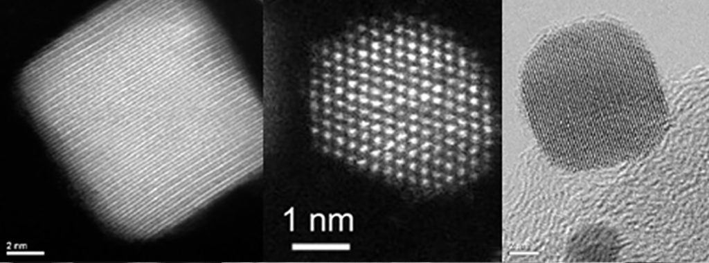
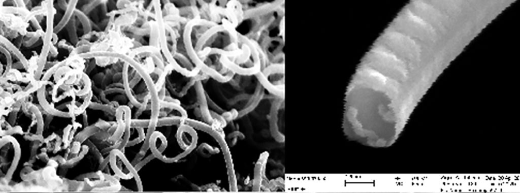
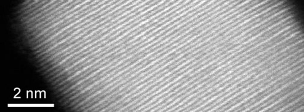
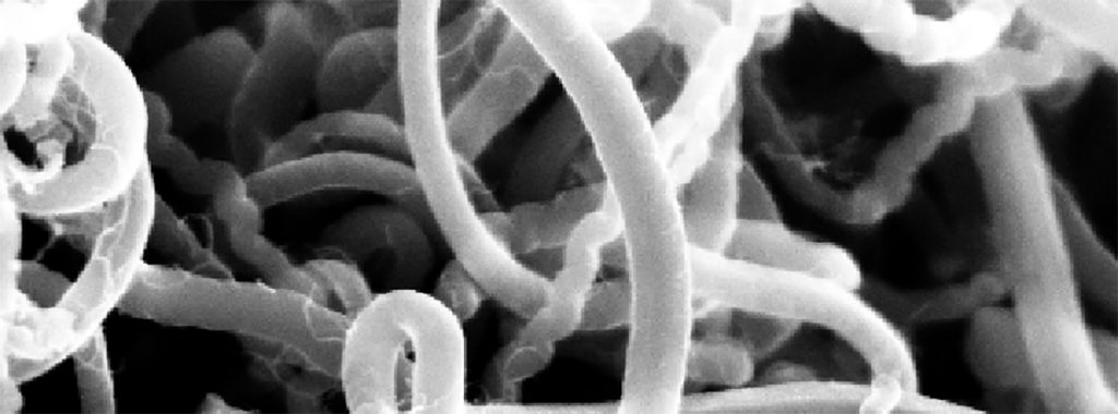
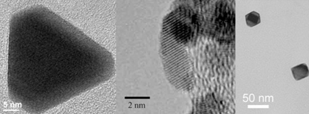
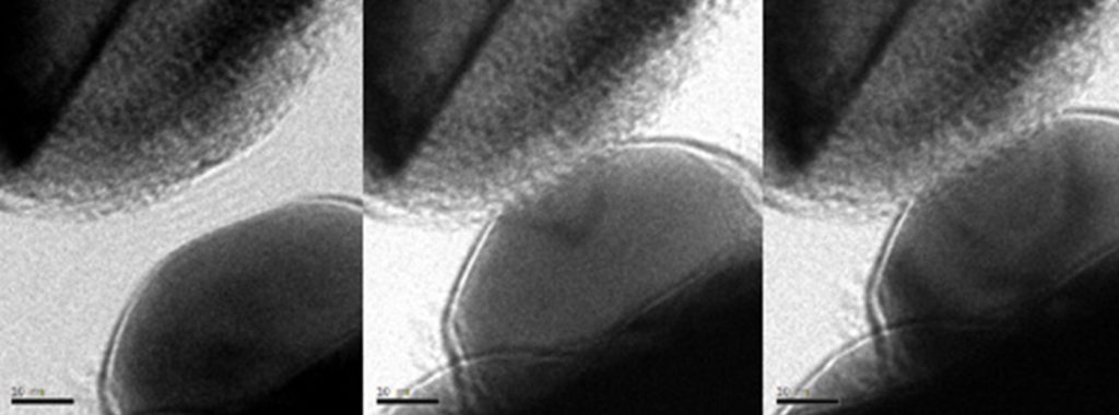
The Atomic Manipulation for Quantum Nanotechnology (AMQN) group is dedicated to creating novel two-dimensional materials and nanomaterials for the state-of-the-art magnetic, electronic, optoelectronic, electrochemical and energy applications. We focus on probing the structure-property interplay of low-dimensional material systems at the atomic scale so as to fulfill atomic manipulation of quantum nanostructures by combining (scanning) transmission electron microscopy, spectroscopy, first-principles calculations and property assessment. Scientifically, special attention is given to a range of defects and interfaces in 2D materials and nanomaterials and how they mediate material property shift at the atomic scale, aiming at tackling fundamental material issues in a broad range of functional material systems. By atomistic design based on first-principles calculations, we aim to develop new functional material systems by a series of preparation methods, e.g. chemical vapor deposition (CVD), chemical vapor transport (CVT), molecular beam epitaxy (MBE), and apply them to fabricate advanced electronic, optoelectronic, and energy devices.

Research lines:
- Development of ferroelectric and ferromagnetic 2D materials
- Development of prototype information storage devices and integrated chips at nanometre scale based on atomically thin 2D materials
- Development of 2D materials for energy storage
- Fundamental research on quantum electron transport in confined systems and ferroelectric and magnetism in reduced dimensions
Projects
Publications
-
Role of sublimation kinetics of ammonia borane in chemical vapor deposition of uniform, large-area hexagonal boron nitride
JOURNAL OF VACUUM SCIENCE & TECHNOLOGY A, 2021Engineering surface electron and active site at electrochemical sensing interface of CN vacancy-mediated Prussian blue analogue for analysis of heavy metal ions
APPLIED SURFACE SCIENCE, 2021Morphology-Tunable Synthesis of Intrinsic Room-Temperature Ferromagnetic gamma-Fe2O3 Nanoflakes
ACS APPLIED MATERIALS & INTERFACES, 2021 -
Mille-Crepe-like Metal Phosphide Nanocrystals/Carbon Nanotube Film Composites as High-Capacitance Negative Electrodes in Asymmetric Supercapacitors
ACS APPLIED ENERGY MATERIALS, 2020Strain-Induced Band-Gap Tuning of 2D-SnSSe Flakes for Application in Flexible Sensors
ADVANCED MATERIALS TECHNOLOGIES, 2020Ultrafine oxygen-defective iridium oxide nanoclusters for efficient and durable water oxidation at high current densities in acidic media
JOURNAL OF MATERIALS CHEMISTRY A, 2020Ultrafine-Grained Porous Ir-Based Catalysts for High-Performance Overall Water Splitting in Acidic Media
ACS APPLIED ENERGY MATERIALS, 2020 -
Strengthening and toughening by partial slip in nanotwinned diamond
CARBON, 2019Competing Interface and Bulk Effect-Driven Magnetoelectric Coupling in Vertically Aligned Nanocomposites
ADVANCED SCIENCE, 2019Magnetism and Optical Anisotropy in van der Waals Antiferromagnetic Insulator CrOCl
ACS NANO, 2019Atomic-scale dynamic observation reveals temperature-dependent multistep nucleation pathways in crystallization
NANOSCALE HORIZONS, 20192D/2D Electrical Contacts in the Monolayer WSe2 Transistors: A First-Principles Study
ACS APPLIED NANO MATERIALS, 2019Effects of Carbon and Boron on Structure and Properties of Austenitic Stainless Steel Coatings Fabricated by Laser Remanufacturing
STEEL RESEARCH INTERNATIONAL, 2019Research on Biodegradable Mg-Zn-Gd Alloys for Potential Orthopedic Implants: In Vitro and in Vivo Evaluations
ACS BIOMATERIALS SCIENCE & ENGINEERING, 2019Inverted Pyramid Textured p-Silicon Covered with Co2P as an Efficient and Stable Solar Hydrogen Evolution Photocathode
ACS ENERGY LETTERS, 2019A highly efficient TiOX (X = N and P) photocatalyst for inactivation of Microcystis aeruginosa under visible light irradiation
SEPARATION AND PURIFICATION TECHNOLOGY, 2019A ternary SnS1.26Se0.76 alloy for flexible broadband photodetectors
RSC ADVANCES, 2019Air-Induced Degradation and Electrochemical Regeneration for the Performance of Layered Ni-Rich Cathodes
ACS APPLIED MATERIALS & INTERFACES, 2019Disassembly of 2D Vertical Heterostructures
ADVANCED MATERIALS, 2019Few-Layer Bismuthene with Anisotropic Expansion for High-Areal-Capacity Sodium-Ion Batteries
ADVANCED MATERIALS, 2019Highly Sensitive Polarization Photodetection Using a Pseudo-One Dimensional Nb((1-x))TixS3 Alloy
ACS APPLIED MATERIALS & INTERFACES, 2019Metallic interface induced by electronic reconstruction in crystalline-amorphous bilayer oxide films
SCIENCE BULLETIN, 2019Nanoscale magnetization inhomogeneity within single phase nanopillars
PHYSICAL REVIEW MATERIALS, 2019Synthesis of low-symmetry 2D Ge(1-x)SnxSe2 alloy flakes with anisotropic optical response and birefringence
NANOSCALE, 2019Vanadium Doping Enhanced Electrochemical Performance of Molybdenum Oxide in Lithium-Ion Batteries
ADVANCED FUNCTIONAL MATERIALS, 2019Microstructure and Mechanical Properties of AZ31 Mg Alloy Fabricated by Pre-compression and Frustum Shearing Extrusion
ACTA METALLURGICA SINICA-ENGLISH LETTERS, 2019Effect of Twinning Behavior on Dynamic Recrystallization During Extrusion of AZ31Mg Alloy
JOM, 2019In Situ Atomic-Scale Observation of Kinetic Pathways of Sublimation in Silver Nanoparticles
ADVANCED SCIENCE, 2019Phase Identification and Strong Second Harmonic Generation in Pure epsilon-InSe and Its Alloys
NANO LETTERS, 2019