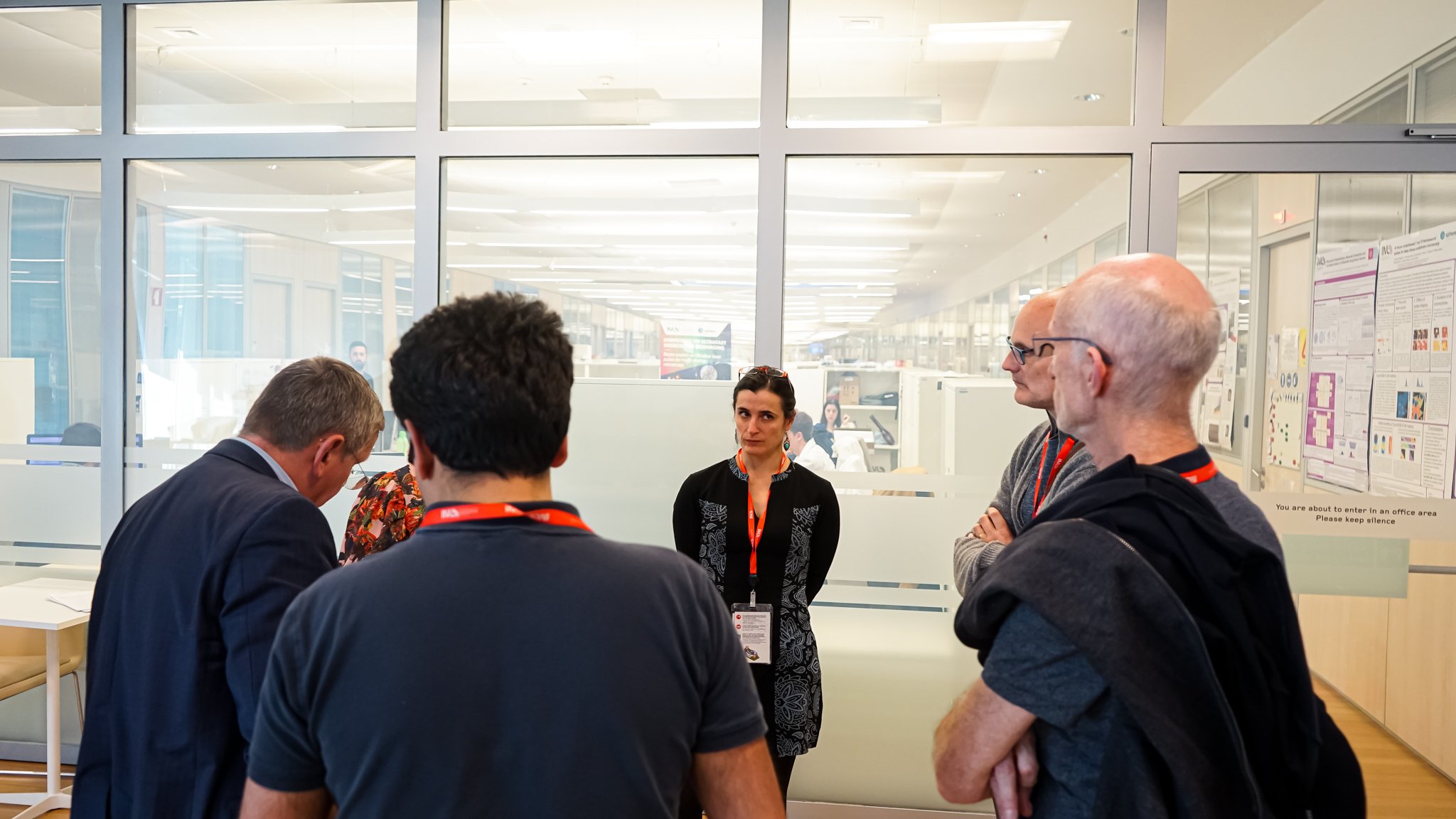
Today, February 2, the CryoEM-PT – National Advanced Electron Microscopy Network for Health and Life Sciences facility was inaugurated at INL – International Iberian Nanotechnology Laboratory, in Braga – Portugal.
The inauguration took place in the presence of Interim Director General – Paulo Freitas, the Scientific Coordinator of AEMIS Facility – Paulo Ferreira, the Alderwoman of Braga – Olga Pereira, the FCT President – Madalena Alves and CCDR-N President – António Cunha.
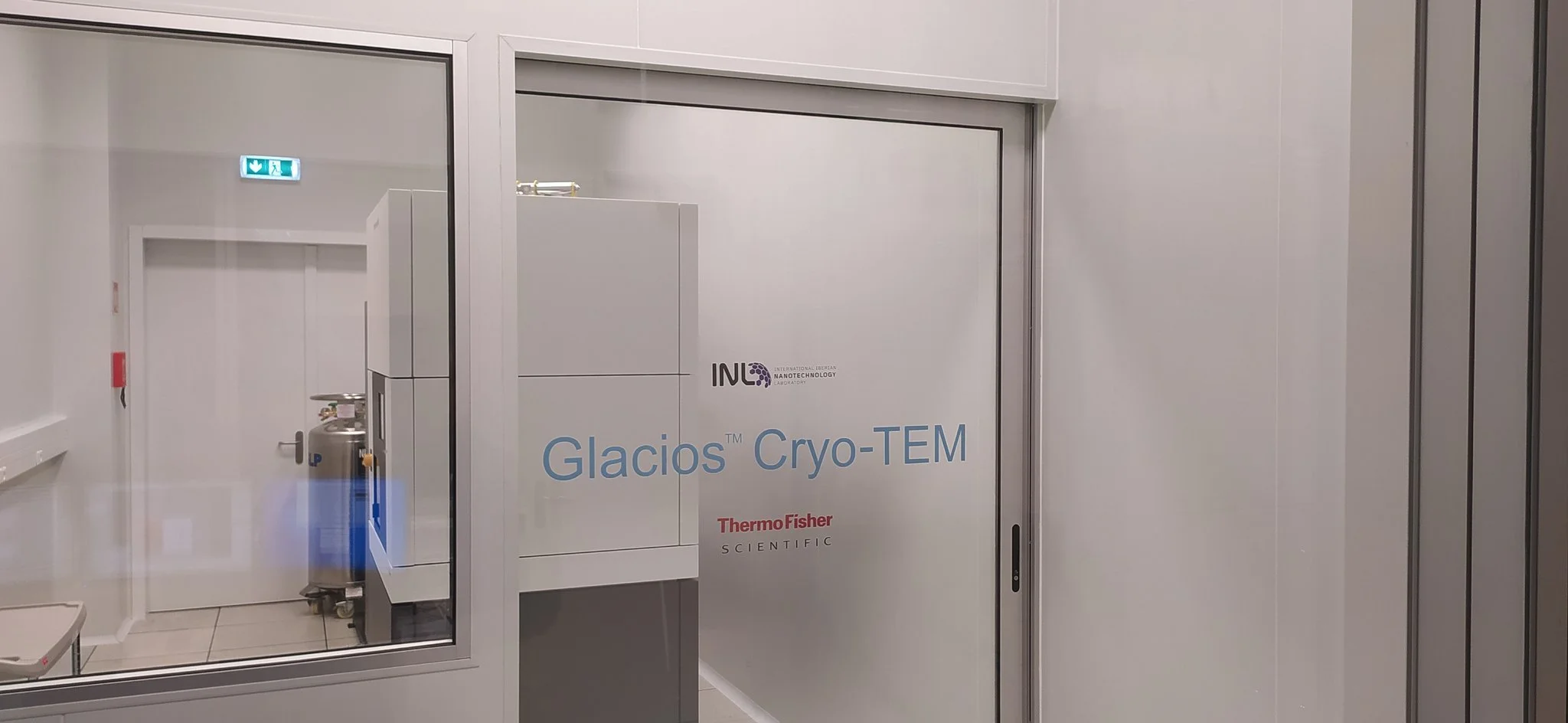
The CryoEM-PT initiative comprises a central node at INL – where a state-of-the-art Cryo-Electron Microscope has just been installed – and several other nodes distributed throughout the country, from North to South. The new infrastructure will soon be available to the scientific and industrial community, particularly in Health and Life Sciences.
Cryo-Electron Microscopy is a state-of-the-art technique fundamental to structural biology and health research, allowing cells and their components to be observed with unprecedented precision. This will allow the study of issues associated with cancer, viral infections, bacterial resistance to antibiotics, Alzheimer’s and Parkinson, as well as the design, development and administration of drugs.
FUNLAYERS twinning EU project kicks off with a workshop
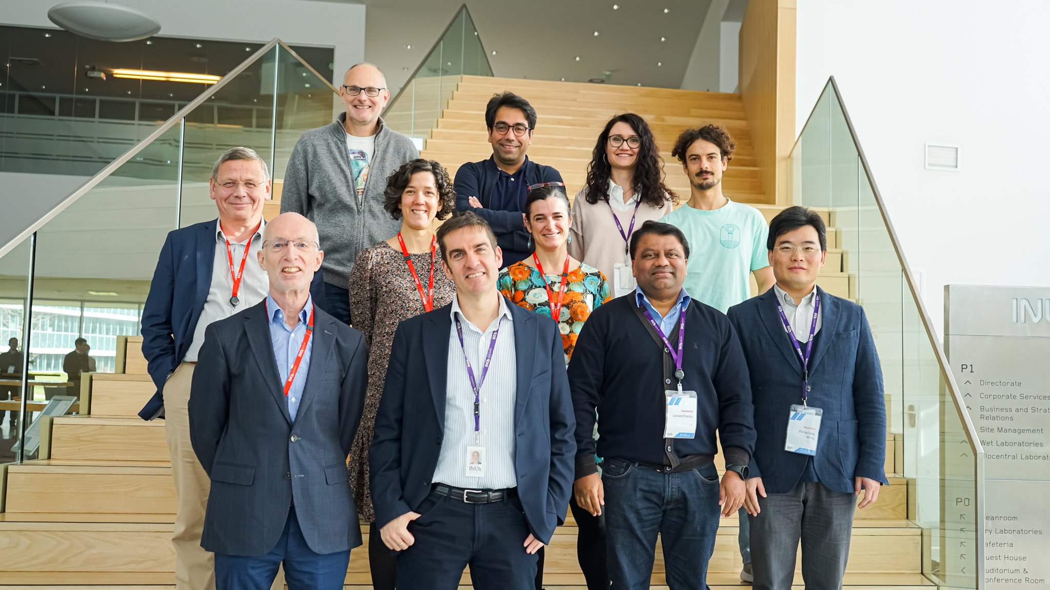
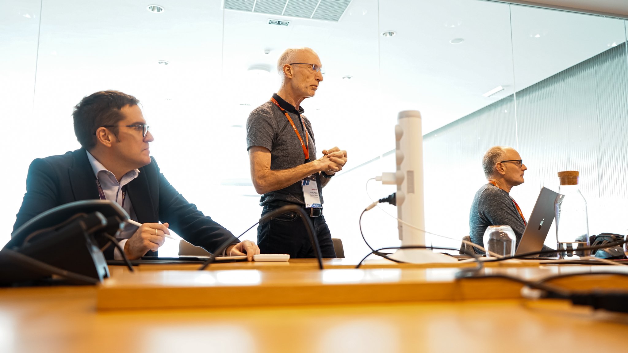
The Functional Layered Materials for Advanced Applications – FUNLAYERS project consists of a twinning initiative aimed to propel INL’s research excellence in the field of layered materials whilst unfolding its tremendous potential applications for energy storage and spintronics in partnership with two world-class European institutions at the forefront of material science – Consortium for the Construction, Equipping and Exploitation of the Synchrotron Light Source (ALBA-CELLS) and the Max Planck Institute of Microstructure Physics (MPG).
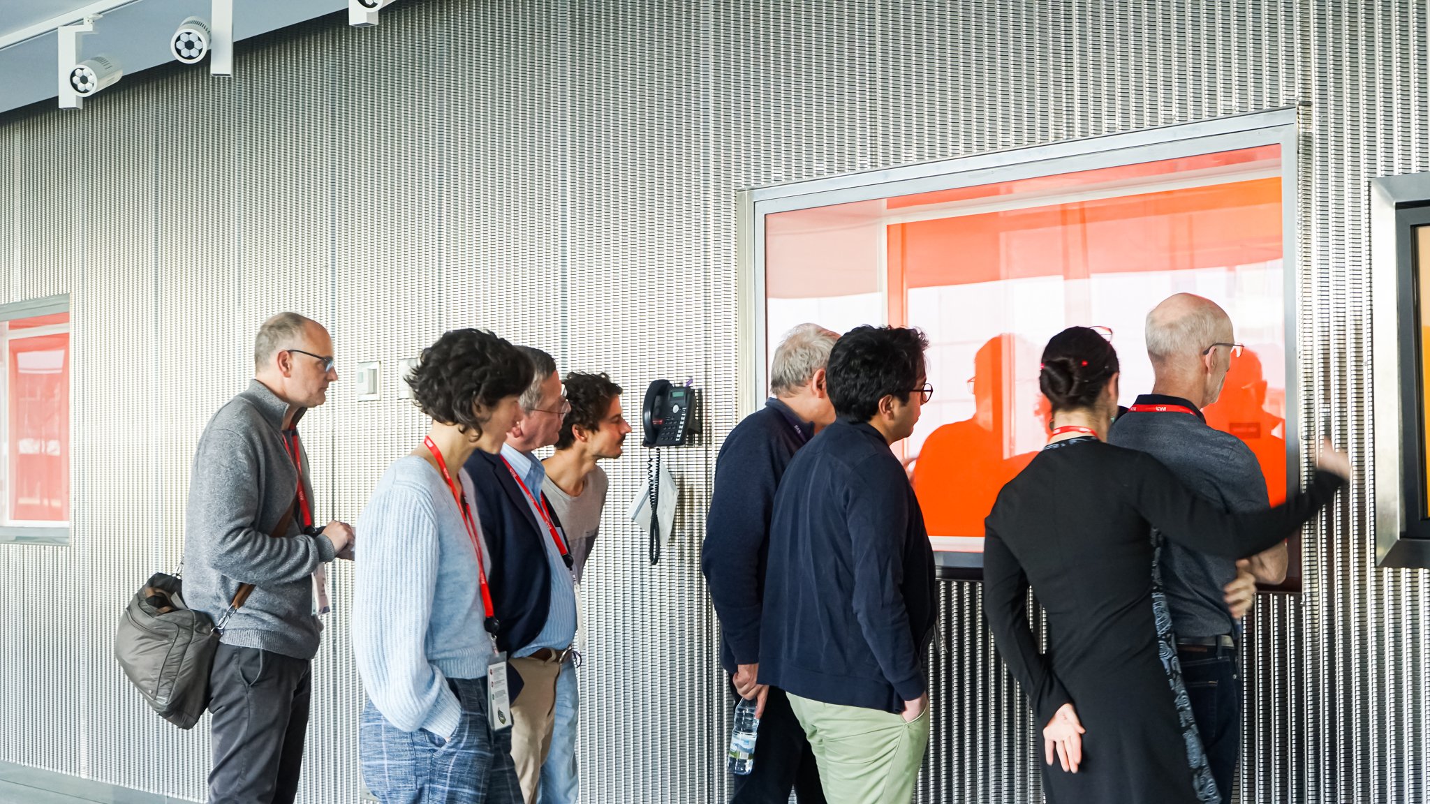
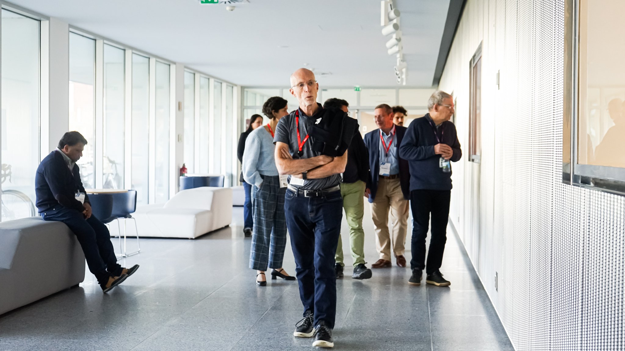
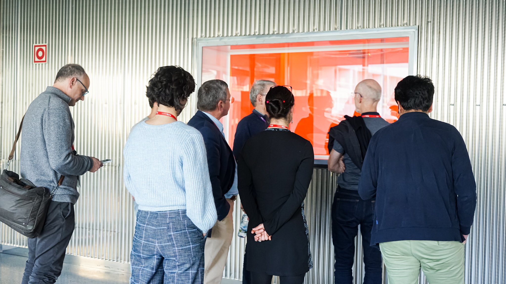
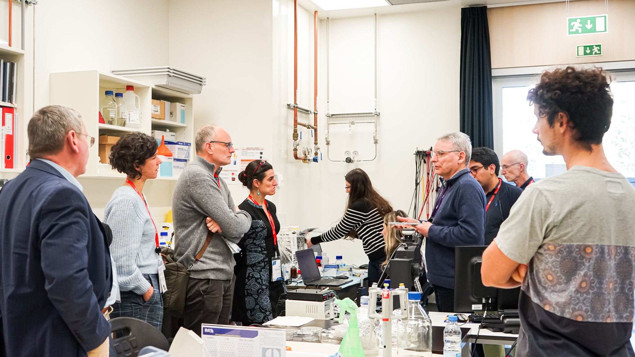
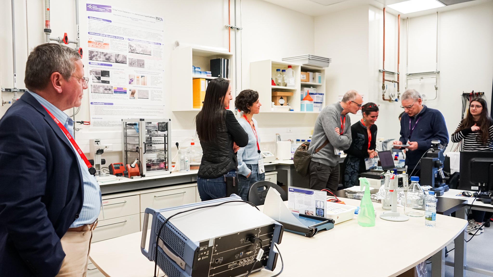
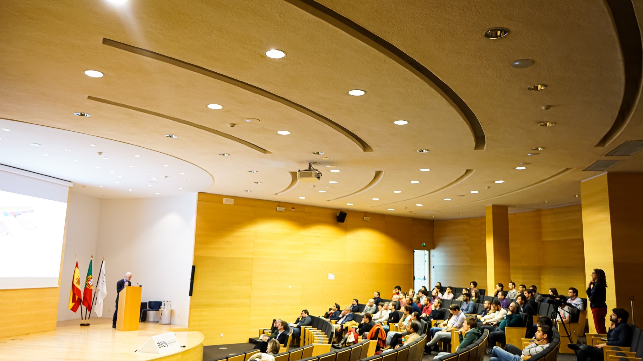
The project kicked off last week in Braga – Portugal, under the coordination of INL – International Iberian Nanotechnology Laboratory together with the other ALBA-CELLS and Max Planck Institute of Microstructure Physics (MPG) teams. The event was a hybrid event, in which the consortium met and discussed the challenges and strategies for the project and how we will work together to strengthen our research in the field of layered materials, capturing future opportunities for joint collaborations in R&I.
During three days FUNLAYERS team organised a workshop and the main goal was to strengthen both the research and the institutional capabilities of INL in the area of Functional Layered Materials and at the same time provide a diagnosis of INL capabilities in two different components – scientific and research management.
On the last day, we were also able to listen to Professor Dr Stuart Parkin – Director of the Max Planck Institute for Microstructure Physics, Halle, Germany, and an Alexander von Humboldt Professor, Martin Luther University, Halle-Wittenberg giving an inspiring talk about his path and work. We heard all about his research interests and the latest developments on spintronic materials and devices for advanced sensors, memory, and logic applications, oxide thin-film heterostructures, topological metals, exotic superconductors, and cognitive devices.
New updates will be shared on the FUNLAYERS website: www.funlayersproject.eu
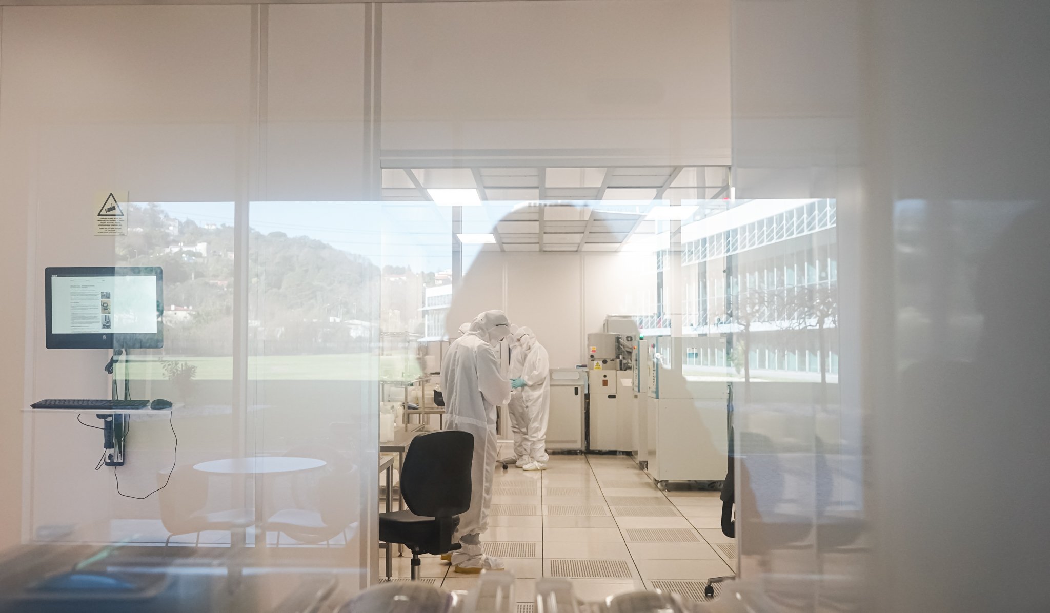
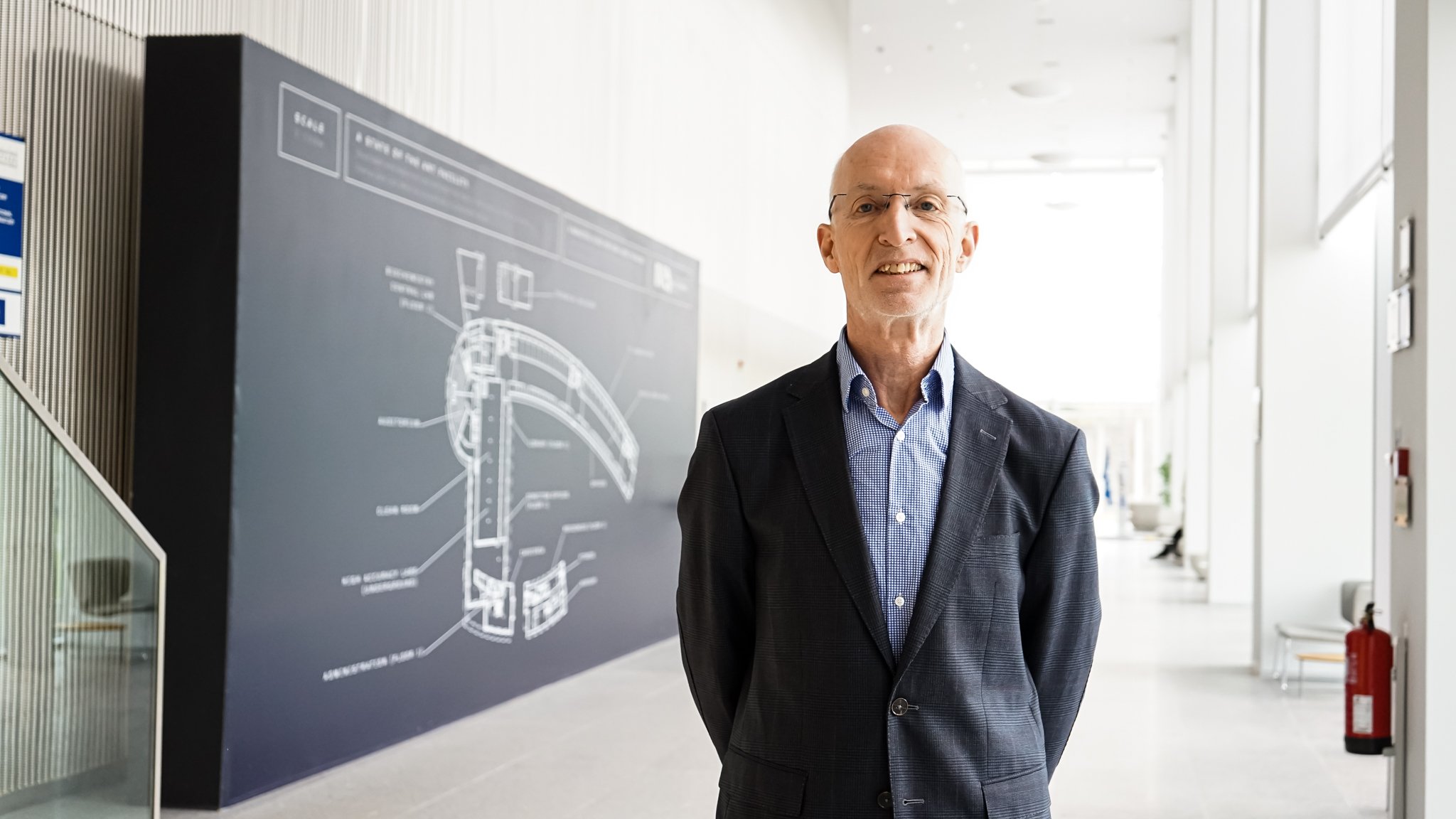
INL inaugurates state-of-the-art Cryo-Electron Microscope that helps to study new diseases
Analysing biostructures down to the atomic level can help to study diseases such as Alzheimer’s or cancer, as well as to develop new therapies. This new type of investigation is now possible from Braga, thanks to the new electronic cryogenic microscope installed at INL – International Iberian Nanotechnology Laboratory.
The acquisition of this equipment is part of the creation of the CryoEM-PT National Network, “an electron microscopy network for life and health sciences”, explains Paulo Ferreira, scientific coordinator of this initiative that opens doors to researchers and companies in Iberia, allowing easy access to state-of-the-art infrastructure and technologies.
The Cryo-Electron Microscopy is a state-of-the-art technique fundamental to structural biology and health research, allowing cells and their components to be observed with unprecedented precision. This type of microscope “uses electrons to look at materials”, which “allows reaching the atomic level”, explains Paulo Ferreira, while “the samples are cooled to the temperature of liquid nitrogen”. The latter is “the advantage of using these instruments”, details the project coordinator since the low temperature prevents “the electron beam from destroying the samples when it interacts with them”. In this sense, the technology it uses is useful for a wide variety of applications, such as “obtaining the three-dimensional structure of biomolecules and viruses such as SARS-CoV-2”, so that “we can develop more effective combat strategies”.
“This opens up a great opportunity to study many therapies and also diseases, for example, Alzheimer’s and Parkinson’s or cancer, as well as the development of new drugs”, which is why not only academic institutions are among the future users, but also companies dedicated to the drug development.
Furthermore, these microscopes are “very computationally demanding; servers with very high speeds and storage capacities are needed”, he explains, since the machine obtains thousands of images per second and in a few minutes generates “a large number of terabytes of data.
Regarding its operation, network users can choose to send the samples directly to the INL – International Iberian Nanotechnology Laboratory team, collaborate directly with its professionals or receive prior training so that they themselves can obtain and analyse the collected data. This technology was awarded the Nobel Prize in Chemistry in 2017 and Paulo Ferreira adds that this is “an instrument considered critical in health and life sciences around the world”.
PITCCH final event happening on March 7, 2023, in Stuttgart, Germany
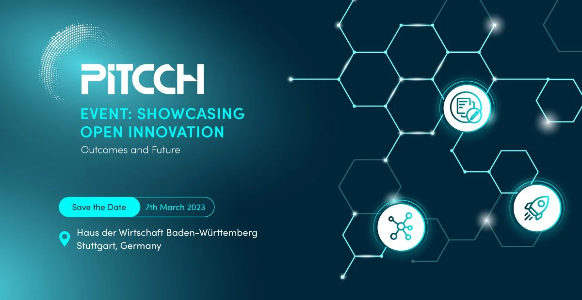
PITCCH project final event will take place on March 7th, 2023, in Stuttgart, Germany.
The purpose is to present results, share good practices from PITCCH collaborations and provide a stage for companies to debate about open innovation strategies and a panel for funding agencies to discuss support programs.
After the opening session with EISMEA Project Officer, DG GROW Policy Officer and PITCCH Project Coordinator, we will welcome our keynote speaker, John Fahlteich, CEO at KETMarket Open Innovation Ecosystem. We will also have a moment to learn from PITCCH collaboration projects. Good practices from Open Innovation projects will be shared by companies that participated in PITCCH.
The first panel of the day “Making Open Innovation work: perspectives from different stakeholders” will gather PITCCH project participants to discuss OI projects and share insights on the perspective of each player. The second panel “Funding Open Innovation: private and public opportunities” will discuss several funding opportunities, both private and public, which could support an Open Innovation framework. A
Tom Fleming is a leading international expert on the creative economy and will be our event host.
PITCCH seeks to accelerate the market uptake of advanced technologies through different sectors. All PITCCH partners are part of an established network ecosystem of multiple stakeholders, from companies to Technology Centres, from private investors to public authorities, and are involved in many international projects, including EU-funded collaborations. The PITCCH consortium consists of four technology centers, INL, the project coordinator, TNO – Innovation for Life, Steinbeis 2i GmbH (S2i) and RINA, and a digital agency, Vitamina.
KESPER, innovative technology that uses a novel class of kesterite materials

The industrial sector is facing a quick growth of clean energy sources. However, it still lacks large-scale energy storage solutions and the availability of clean fuels with high energy value. It is crucial to reduce energy consumption, by increasing the efficiency of energy systems and by promoting their greenization.
KESPER – The kesterite-based Photoelectrodes for Water and Nitrogen Reduction project proposes an innovative technology that uses a novel class of kesterite materials avoiding the use of critical raw materials for the generation of renewable gases. Kesterite, a greenish-black mineral, presents several forms and compositions; however, this also makes it extremely versatile with adaptable features.
Kesterite semiconductor compounds can be alloyed with several elements and can be used to develop environmentally-friendly photoelectrodes, which have the capability to tune their energy bandgap depending on their elemental composition among other tuneable properties.
Although this material has only been extensively studied over the past decade, when used in thin-film solar cells, it can deliver light-to-power conversion efficiencies of close to 13%, demonstrating its huge potential for the clean energy sector. In KESPER, we are combining the advantages of kesterite together with tailored surfaces, coatings and interfaces, towards the development of low-cost, earth-abundant, and easily recyclable photoelectrodes. Our final demonstrator will be developed with scalable techniques, following life-cycle thinking, and without requiring critical or toxic materials, suitable for both water and nitrogen reduction.
This unique project is managed by the M-ERA.NET network, and brings together a strong consortium between INL – International Iberian Nanotechnology Laboratory, Hasselt University, Interuniversity Micro Electronics Centre and the Technical University of Denmark, to develop better alternatives for clean energy production.
Next Page » « Previous Page -->The industrial sector is facing a quick growth of clean energy sources. However, it still lacks large-scale energy storage solutions and the availability of clean fuels with high energy value. It is crucial to reduce energy consumption, by increasing the efficiency of energy systems and by promoting their greenization.
KESPER – The kesterite-based Photoelectrodes for Water and Nitrogen Reduction project proposes an innovative technology that uses a novel class of kesterite materials avoiding the use of critical raw materials for the generation of renewable gases. Kesterite, a greenish-black mineral, presents several forms and compositions; however, this also makes it extremely versatile with adaptable features.
Kesterite semiconductor compounds can be alloyed with several elements and can be used to develop environmentally-friendly photoelectrodes, which have the capability to tune their energy bandgap depending on their elemental composition among other tuneable properties.
Although this material has only been extensively studied over the past decade, when used in thin-film solar cells, it can deliver light-to-power conversion efficiencies of close to 13%, demonstrating its huge potential for the clean energy sector. In KESPER, we are combining the advantages of kesterite together with tailored surfaces, coatings and interfaces, towards the development of low-cost, earth-abundant, and easily recyclable photoelectrodes. Our final demonstrator will be developed with scalable techniques, following life-cycle thinking, and without requiring critical or toxic materials, suitable for both water and nitrogen reduction.
This unique project is managed by the M-ERA.NET network, and brings together a strong consortium between INL – International Iberian Nanotechnology Laboratory, Hasselt University, Interuniversity Micro Electronics Centre and the Technical University of Denmark, to develop better alternatives for clean energy production.