Micro and Nanofabrication
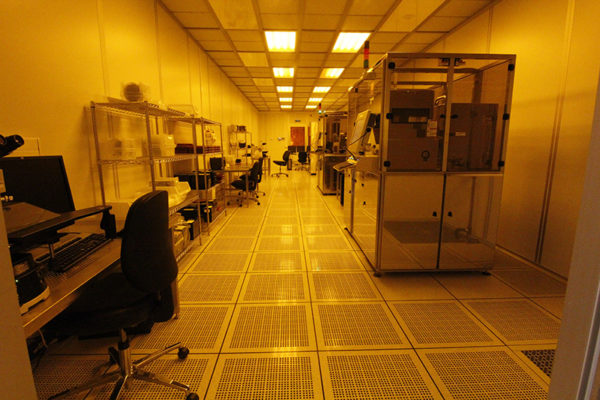
The Micro and Nanofabrication (MNF) Facility operates a Class 100 cleanroom with a total area of 1,200 m2. It offers access to a state-of-the-art equipment suite for micro- and nanofabrication solutions on 200 mm diameter wafers with applications ranging from electronics, medical devices, microfluidics, energy and sensors.
Besides training and supporting users, the MNF facility at INL is a key partner for contracted research and services from the early stage of the design concept up to the last phase of the first prototype. It unfolds from device design, process integration and development to expert process engineering on the latest core technologies.
The MNF facility is also prepared for small pre-production series, including multi-project wafers (MPW), facilitating technology transfer to industry for research laboratories, start-ups, SMEs and large companies.
Core fabrication areas
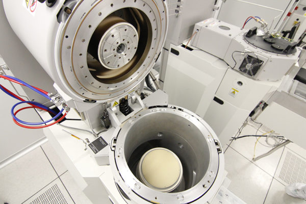
Multi-target Singulus sputtering tool for magnetic multilayers (Timaris MTM)
Multi-target confocal sputtering tool (Kenosistec)
Metallization Singulus sputtering tool for Al, TiW(N) and Al2O3 (Timaris FTM)
EasyTube 3000 Graphene CVD furnace system
SPTS MPX CVD system for oxides, oxi:nitrides and a-Si:H deposition
PECVD (800ºC) systems for CNT and carbon layers deposition tool (MicroSys 400 from Roth & Rau Microsystems)
Thin film silicon CVD system (hotwire and radio-frequency assisted, doped and intrinsic Si layers)
Cu Electroplating (AMMT GmbH)
Atomic Layer Deposition (Beneq TFS 200)
Broad Beam ion milling with SIMS end point detect (Nordiko 7500)
Fluorine-based reactive ion etch system for oxides / nitrides (SPTS APS)
Chlorine-based reactive ion etch systems for metals (SPTS ICP and SPTS C2L ICP)
Silicon Deep reactive ion etching system (SPTS Pegasus)
Plasma asher (PVA TEPLA M360)
TMAH / KOH Si etch tanks (AMMT GmbH)
Multiple fume hoods and wet benches for chemical processes (Quimipol)
Oxide vapour etch release system (SPTS/PRIMAXX uEtch)
XeF2 isotropic Si etch system (Xactic X4)
Supercritical CO2 point dryer (Tousimis)
E-beam lithography tool (Vistec 5200 ES 100 kV)
Nanoimprint Lithography (Obducat Eitre8)
Direct write laser lithography (Heidelberg DWL 2000)
Mask aligner (Karl Suss MA BA model)
Optical resist track (Karl Suss Gamma Cluster)
E-beam resist track (Karl Suss Gamma Cluster)
Multiple ovens, including vapour priming
Coater and hotplates for substrates up to 300 mm (SCS/EMS)
Chemical Mechanical Planarization (Logitech ORBIS)
Dicing saw (Disco DAD 3500)
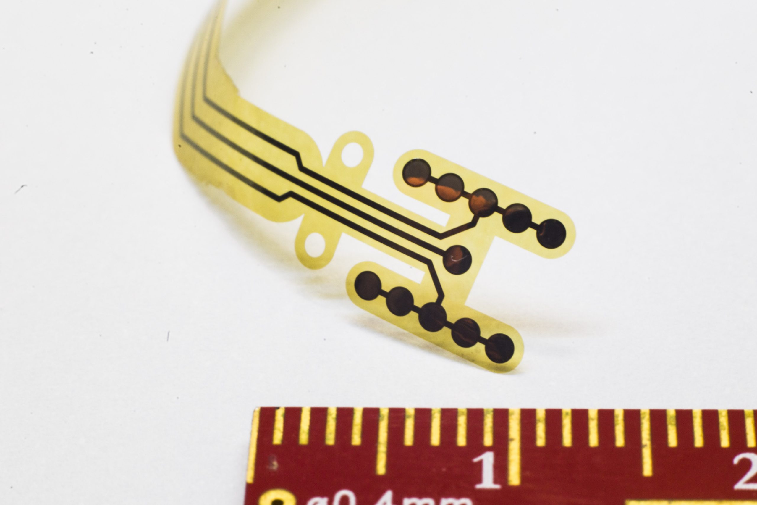
Wire Bonder / Aluminium Wedge, Pick and Place (TPT HB)
Wire Bonder / Gold ball bond (TPT HB)
Pick and place (Finetech Fineplacer Sigma)
Advanced desktop research printer (LP50 Roth & Rau B.V.)
Magnetic Annealer (TEL, MATR 2000)
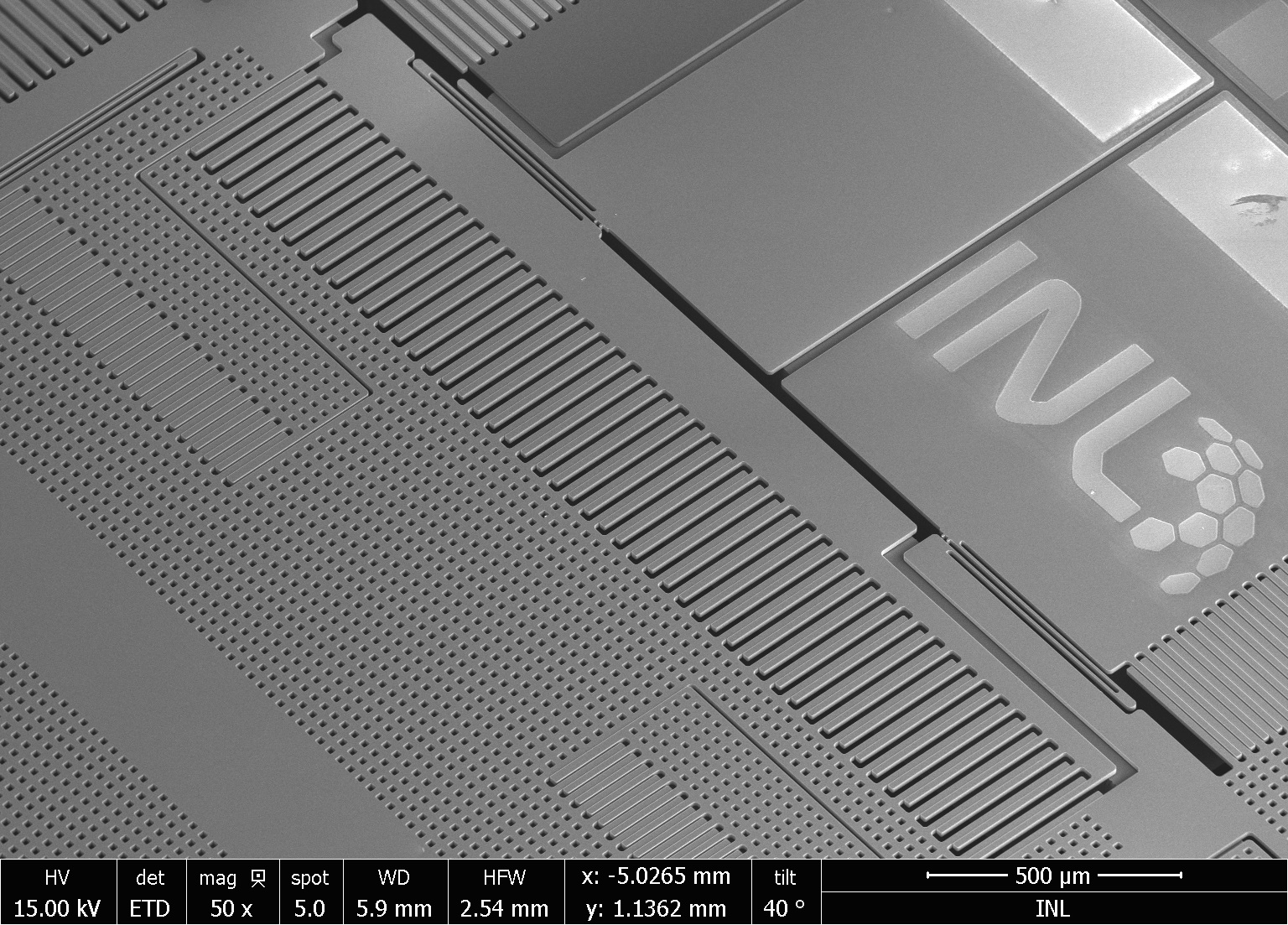
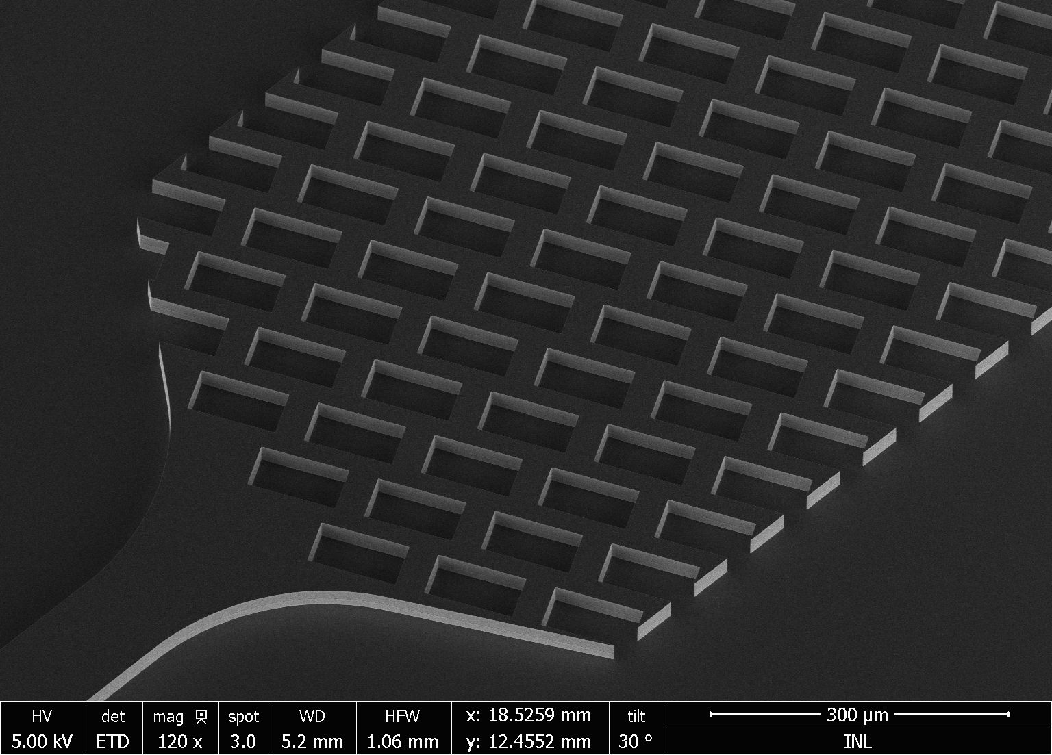
High-resolution SEM (NanoSEM, FEI)
Contact profilometer (KLA TENCOR P-16+)
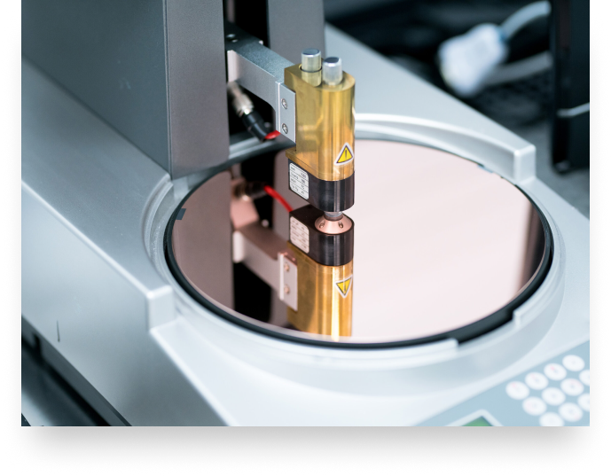
Resistivity mapper (AITCO)
Optical profilometer/ellipsometer (OPM hyperion with confocal sensor / Ocean Optics NanoCalc XR)
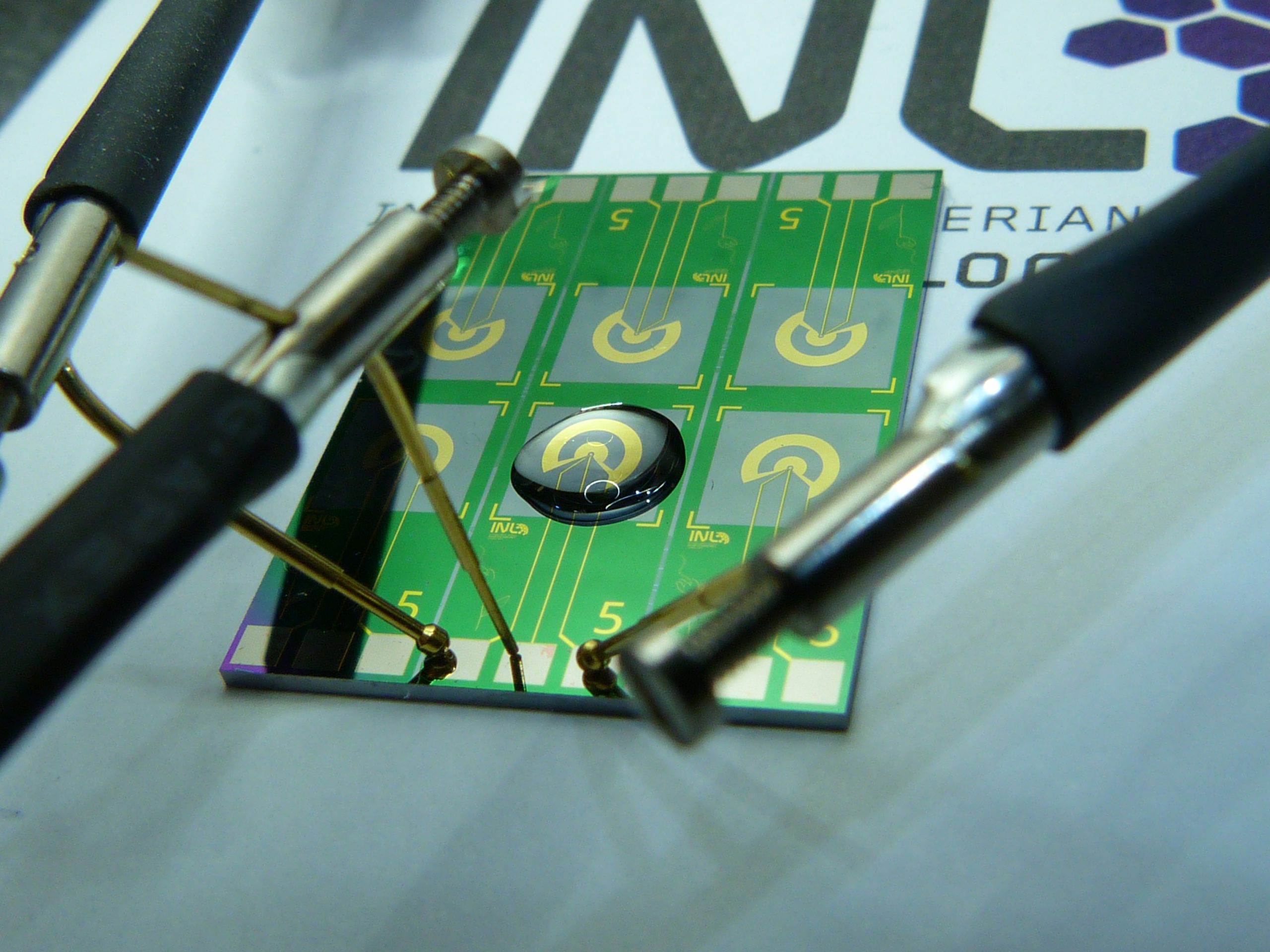
Multiple automated wafer probers for electrical testing and others
Manual and motorized optical microscopes for Automatic Optical Inspection