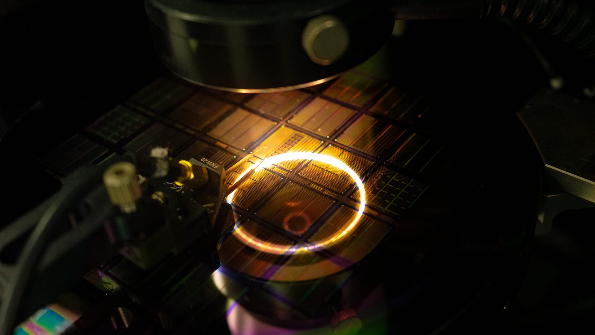
Hybrid CMOS Spin Chips
The ability to integrate the Spintronic devices in standard CMOS wafers is a fundamental step for large-scale production, dissemination and commercialization of the research produced at INL. Furthermore, Spintronics and CMOS technology can be integrated to create hybrid devices with functionalities, which are not available in any of the two individual technologies.
A first test of this integration was made with a relative high density matrix of magnetic sensors used to sense the magnetic fields. An array of 256×256 devices, which is equal to 65536 MTJs (micro-sized sensors), on a CMOS chip of 4×6 mm2 was successfully integrated. The CMOS design allowed addressing each individual element, sweeping the full matrix to form a magnetic field image and showed a very high success rate of the integration (>90%). The topology of such matrix is very similar to the topology used in non-volatile memory applications (MRAM), but rather than using bi-stable elements, this matrix used magnetic sensors with an analog output.
CMOS1_new – “A first test of this integration was made with a relative high density matrix of magnetic sensors used to sense the magnetic fields. An array of 256 x 256 devices, which is equal to 65536 MTJs (micro-sized sensors), on a CMOS chip of 4×6 mm2 was successfully integrated.”
CMOS2_new – “same”
CMOS3_new “same”
CMOS4_new- “An overview of the measured TMR values of the individual devices. Black points mark devices that are not working. The CMOS design allows addressing each individual element, sweeping the full matrix to form a magnetic field image, showing a very high success rate of the integration (>99%)”
spintronicsP4_1- “The ability to integrate the Spintronics devices in standard CMOS wafers is a fundamental step for large-scale production, dissemination and commercialisation of the research performed at INL. Furthermore, Spintronics and CMOS technology can be integrated to create hybrid devices with functionalities that would otherwise not be available with any of the two individual technologies.”
Such device can capture of magnetic images which are useful in applications such as cell histology. Magnetic nanoparticles attached to specific receptors in the cell surface can be imaged and provide useful information about specific biological systems. (Image spintronics P4)