INL facilities open to external users
November 9, 2012
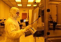
The International Iberian Nanotechnology Laboratory provides 22,000 m2 of laboratory space and state-of-the-art equipment for various research areas. INL scientific facilities are fully operational since the beginning of 2011 and cleanroom processes and laboratory equipment are now available for external users.
The cleanroom provides class 100 and class 1000 laboratory space dedicated to nanolithography, photolithography, wet process, planarization, reactive Ion etching, deposition, and analytical instrumentation for process and device characterization. A separate biology bay completes cleanroom key capabilities.
The central Biology and Biochemistry facility provides support for groups developing research in these areas, including specific facilities for molecular biology, microbiology, bio-imaging facility.
The high accuracy laboratories offer a detailed structural characterization of thin films, interfaces, nanostructures, and biological structures. Available techniques include atomic force microscopy, surface analysis by XPS, electron microscopy including a probe corrected TEM, FIB and environmental SEM.
Other support labs provide state-of-the-art equipment for optical imaging, spectral ellipsometry, magnetometry, radiofrequency device characterization, MEMS, and nanochemistry/spectroscopy.
External users can check equipment and process availability at INL website, as well as the contact person for the particular item. Conditions of use are as follows:
1 -external users coming to INL within approved collaborative projects (FCT, CSIC, European union, companies, university/research center-INL protocols, others)
– Users will get temporary user status at INL and will perform/participate in the measurements, processes, research specified in the project always in collaboration with the project representative at INL. INL costs will be internally charged to the research project.
2 -external users requesting particular work/service or equipment use outside any collaborative framework
– Users must supply a brief description (maximum one page) of the work/service required and send it to the proper equipment/process contact person
– if work/service is approved, the work/service invoice will be prepared, and the respective work/service order needs to be received at INL prior to work execution
-after work/service completion, INL will invoice the ordering entity for the work done.
The equipment was cofinanced the under the Portuguese North Regional Program “ON.2 – O Novo Norte”, Operations Norte-07-0162-FEDER-000002 and NORTE-07-FEDER-000045.
Equipment Overview
X-ray thin films/reflectometry
Small angle X-ray scattering (SAXS)
Atomic force microscope – materials
Atomic force microscope – bioscience
X-ray photoelectron spectroscopy
Service enquires (including mask fabrication) paulo.freitas(at)inl.int
Direct write laser lithography
CNT deposition tool (PEV, 800C)
Chemical mechanical Polishing and Planarization Tool
Multitarget sputtering tool (200 mm)
Multitarget confocal sputtering tool
Metallization sputtering tool (Al, TiWN, Al2O3)
Broad beam ion milling with SIMS end point detection
PECVD oxides, oxynitrides, and a-Si:H
Oxide vapour etch Ion release system
Resistivity mapper – four probe
Optical profilometer/ellipsometer
Packaging Laboratory
Optical Imaging, Spectral ellipsometry, others
Life science confocal microscope
Multifunctional Inv. microscope for life sciences
Magnetometry, RF and MEMS laboratories
Magnetic annealer (=-2T, 0-400C)
CIPT tester (in plane and out of plane field)
Electronic Support
Service enquires (IC design, PCB layout, etc…) joao.piteira(at)inl.int
Micro volume Fluorospectrometer
Gel Imaging (fluorescence and chemiluminescence)
Nanochemistry/Spectroscopy Laboratories
Automated gas sorption analyser/pore size-surface area
Thermogravimetry and differential Scanning Calorimetry
Gas analyser system/Mass Spectrometer
Dynamic Light Scattering (DLS) and Zeta Potential (ZP) measurement system
Optical Emission Spectrometer (ICP-OES)
Fluorescence life time Spectroscopy
Atomic Layer Deposition (ALD) System
Solar Illumination – IV solar cell test
Quantum efficiency measurement system (QEX10)
Controlled intensity Modulated Photocurrent/Photovoltage Spectrometer (CIMPS)