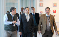
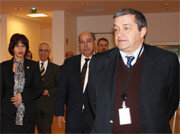
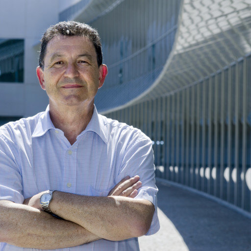
FINLAND OPEN TO ACADEMIC AND INDUSTRIAL COLABORATION IN NANOTECHNOLOGY

FINLAND OPEN TO ACADEMIC AND INDUSTRIAL COLABORATION IN NANOTECHNOLOGY

The Director-General of the International Iberian Nanotechnology Laboratory (INL), José Rivas, was pleased with the interest shown by the Finish academic and industrial institutions visited during the stay organized by the President of the Republic of Portugal, Aníbal Cavaco Silva, to Helsinki, last week. Erkki Ormala, Vice-President for Business Environment at Nokia, one of the world leaders in communication technologies, showed interest in visiting the International Iberian Nanotechnology Laboratory, with its headquarters in Braga. The future visit of Nokia representatives will allow establishing collaborations in strategic areas like electronic devices and sensors. INL also visited Micronova, the Centre for Micro and Nanotechnology Nanofabrication, on the Otaniemi Campus of Aalto University, where the delegation was hosted by Ilkka Niemela, Dean of the School of Science. The Research, Technology and Development activities of the finish nanotechnology cluster were made known through several presentations. From these presentations, Prof. Rivas concluded that there are groups of excellence working on nanomedicine and materials research. «The academic quality is remarkable and the way research and industry are connected in an example to be considered», said José Rivas. One of the strategic goals of INL is to stand out as a scientific organization of excellence, with an […]

Read more
INL installs LPX Pegasus ASE, a Deep Silicon Etch (DRIE) with a broad range of challenging applications

INL installs LPX Pegasus ASE, a Deep Silicon Etch (DRIE) with a broad range of challenging applications

Advanced Silicon Etch (ASE) is a deep reactive ion etching (DRIE) technique used to rapidly etch deep and high aspect ratio structures in silicon. LPX Pegasus is the continuation of STS’ Advanced Silicon Etch (ASE) technology. Through an in-depth understanding of the Bosch process and with the required hardware, Pegasus is able to provide excellent profile control and selectivity. The increased etch rate and improved uniformity lead to higher throughput and device yield, resulting in increased productivity. This inductively de-coupled plasma (IDP) system uses fluorine-based gases for anisotropic deep silicon trench etching. The 13.56 MHz RF power supply produces high-density, low-pressure, low-energy plasma. This type of plasma allows high selectivity and aspect ratio etching for depths greater than 150 microns and has an expected etch rate better than 15 microns/ min. Used primarily for MEMs devices, the typical materials used in this etcher are silicon wafers covered with photoresist and thin films of silicon dioxide and silicon nitride. The performance improvements that Pegasus brings have numerous benefits for research as well as for end-users. At the moment, the tool is being installed in the INL’s facilities and it is expected that the final validation process will take place the first […]

Read more
INL project presented in Mexico during NanoMex’10

INL project presented in Mexico during NanoMex’10

In pursue of INL’s outreach program, Jose Rivas, Director General (DG) of the INL, attended the“Simposio: Nanociencias y Nanotecnología” at UAM in Mexico City, 15-16 November and the NanoMex’10 which is the Third International and Interdisciplinary Nanoscience and Nanotechnology Meeting, organized by the National Autonomous University of Mexico (UNAM), in Cuernavaca City (Morelos) 17-19 November. In this meeting, the DG of the INL made the most of the encounters to present the INL and to contact leading important Mexican scientists in the field of Nanotechnology. The goal of NanoMex’10 is to stimulate high-quality interdisciplinary dialogue on the advance, promises and implications of nanoscience and nanotechnology in order to enrich the national decision-making concerning the distribution of benefits, maximization and definition of responsibilities and, the minimization of unnecessary and unwanted costs. It is an initiative nano-UNAM, a group initially formed by the Centre for Interdisciplinary Research in Sciences and Humanities, the Center for Nanoscience and Nanotechnology, the Center for Applied Sciences and Technological Development and the Environmental Nanotechnology University Program. Since 2009, nanoUNAM is conformed by 11 UNAM’s entities and a research university program.

Read more
1 157 158 159