INL researchers develop a novel compact and low-cost microLED chip
April 21, 2023
Light-emitting diode chips, commonly known as LEDs, are semiconductor light sources that are used in smartphones for displays, automotive lighting, medical devices, sensors and optical communications. LEDs typically combine a large p-type doped semiconductor layer (layer with faulty conduction electrons; these lack of conduction electrons behave as positive charges called holes) with an n-type doped semiconductor layer (layer with abundant conduction electrons), forming a p-n junction. When a sufficient voltage is applied, electrons and holes move across the p-n junction and electrons recombine with holes releasing energy in the form of light.
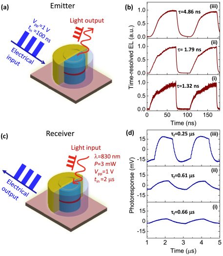
Temporal electrical and optical response of the microLED. (a) The emitter configuration for electro-optical modulation. (b) The time-resolved electroluminescence (EL) as a function of the forward bias voltage: (i) 2 V, (ii) 2.5 V, and (iii) 3 V for 1 V, 100 ns input electrical pulses. The determined decay lifetime (τ) is indicated for each bias condition. (c) The receiver configuration for optoelectrical modulation. (d) The photocurrent response to illumination by a laser source (𝜆∼830nm�∼830nm) driven by 1 V, 2 µs square-wave voltage pulses. The photocurrent was measured as a function of the forward bias voltage: (i) 2 V, (ii) 2.6 V, and (iii) 3.5 V. The photoresponse fall time (𝜏𝑓��) indicated for each bias condition is determined as the time between 10% and 90% of the maximum photocurrent.
The layered p-n junction structure is one of the most well-established semiconductor optoelectronic modern chip technologies that revolutionized the development of LEDs, lasers, and photodetectors. However, given the recent miniaturization of light-emitting and photo-detecting devices, such as nanoscale LEDs and nano-photodetectors, the use of p-type semiconductors adds significant complexity and associated costs to the device’s manufacture.
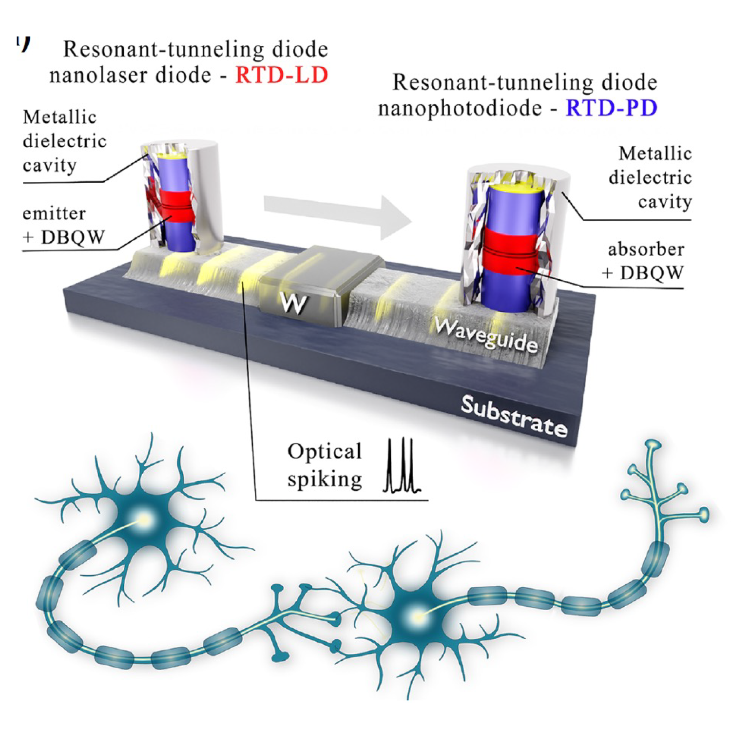
In this recent work, INL researchers in collaboration with the University of Lisbon, present a novel microLED chip that does not need p-type semiconductor layers. Furthermore, the developed microLED also has the astounding ability to work as both a light emitter and a detector, in the same circuit.
Bruno Romeira, the leader of this study, explains that “the architecture of the device provides a compact and low-cost microLED chip with seamless integration of multi-capabilities (electroluminescence, photoresponse and negative differential conductance – electrical on-chip gain), under identical operating forward voltage conditions”.
The findings of this study pave the way for a wide range of low-cost applications in on-chip light-emitting and light-receiver systems, of key importance for imaging, sensing, signal processing, data communications and neuromorphic computing AI applications.
This study was funded by the European Union, Horizon Europe, under project 828841 – ChipAI, and project 101046790 – InsectNeuroNano. You can find the full article here: https://doi.org/10.1364/OPTICA.476938.