
Interview with Leonard Deepak Francis, INL Group Leader
August 24, 2020
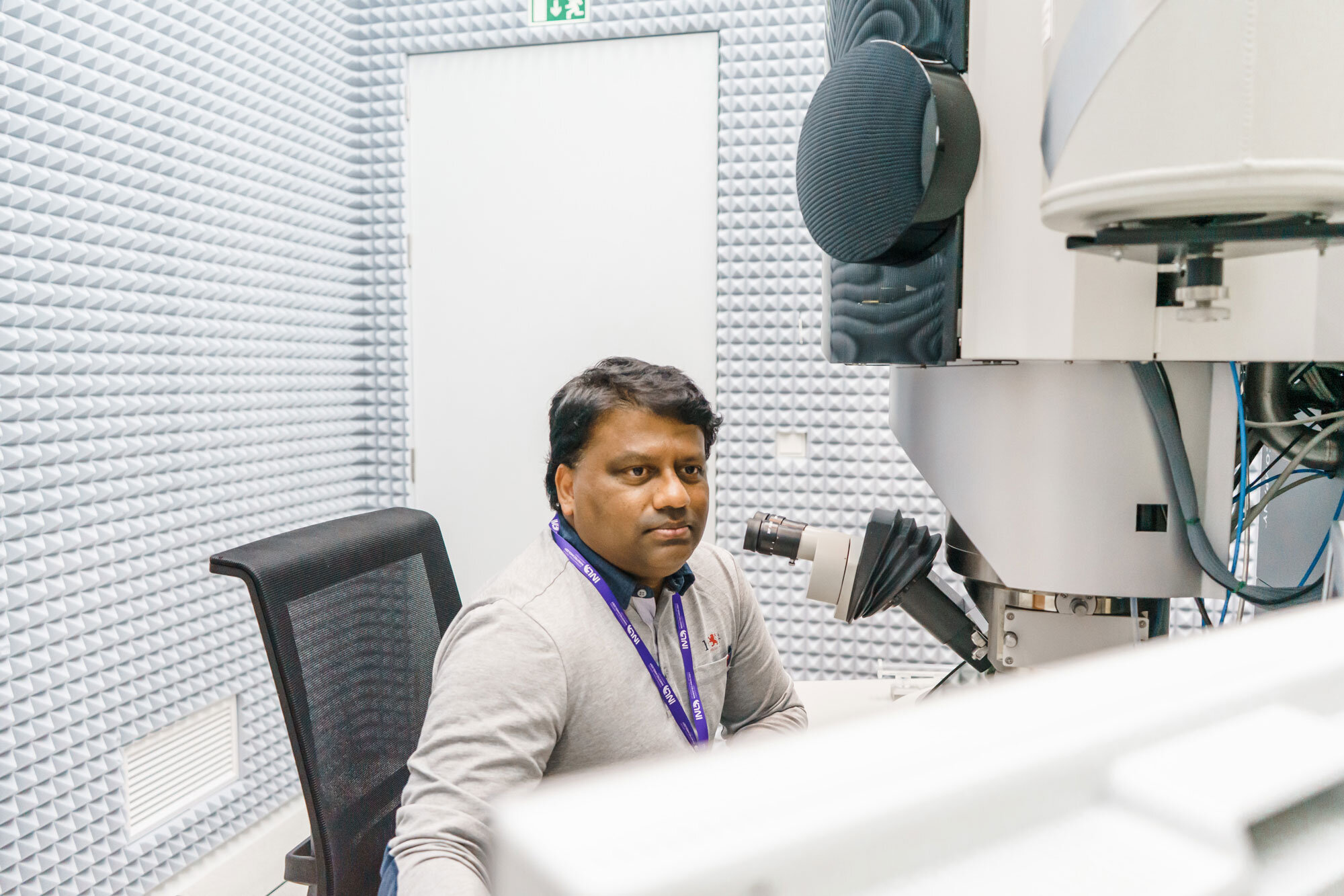
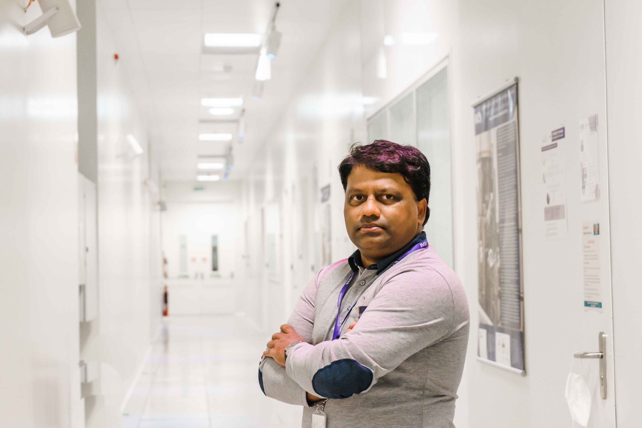
Leonard Deepak Francis is the group leader of the Nanostructured Materials Group at INL. His research is focused on the use of advanced electron microscopic techniques for the study of materials/nanomaterials for various applications, as well as in the study of physical phenomena and dynamics at the atomic-scale.
You have been working at INL since 2009, how was your journey so far and what were the most important projects you’ve worked in?
I was recruited by INL in the summer of 2008 and started to work as a research fellow at the University of Texas-San Antonio (UTSA), U.S.A in January 2009. This stay lasted until March 2011. During the course of this period, the INL building was being constructed and I had a chance to visit INL for the first time in the year 2010 when the constructions were ongoing. During my time at UTSA, I had the possibility to work on the first commercially available Aberration Corrected Scanning Transmission Electron Microscope (AC-STEM) from the company JEOL that was installed then at UTSA. With this microscope, it was possible to achieve an unprecedented resolution of 80 pm (pm – picometres) which enabled visualization of atoms directly which was quite exciting. The training that I received on this microscope at UTSA was very useful for the work that I am currently doing at INL.
Subsequent to my stay at UTSA, I came to Portugal and started to work at INL in Apr 2011. I was involved in the early discussions associated with the acquisition of the microscopes for INL, visited the FEI (now Thermo Fischer) factory at Eindhoven, to test the microscopes before their formal installation at INL. During the course of the year 2011-2012, the High Accuracy Labs were being set-up and I was associated with the installation of the first batch of electron microscopes – three of the electron microscopes that arrived during that period – the Quanta Environmental Scanning Electron Microscope (ESEM), the dual-beam Focused Ion Beam (FIB) and the first of the Titans – The ChemiSTEM. The ChemiSTEM which is a probe aberration-corrected microscope has a resolution of 80 pm with a very special detector for chemical analysis called the Super-X detector, one of the very first microscopes with this feature to be installed at INL at that time.
During the course of the year 2015, the second batch of microscopes was installed namely the JEOL Transmission Electron microscope and the Themis double corrected aberration-corrected TEM/STEM. It has been indeed exciting to be part of this journey since the very beginning and see how things have evolved over the years: at the microscopy facility with which I am associated closely and at INL which has transformed from the very beginning until what it is today. I cannot believe that it is already more than 10 years now that I am at INL.
This unique capability of microscopes that we have at INL has helped immensely in our work over the course of the years. We were able to show very early on combined structural-morphological-chemical analysis of heterostructures in three-dimension (3D), employing EDS-Tomography (EDS- Energy Dispersive Spectroscopy). This was possible as I mentioned before due to the unique Super-X capability that we have with the ChemiSTEM. We routinely employ the high-end electron microscopy available at INL to study the atomic structure of catalysts and energy-related materials an important and current area of our work at INL. The FIB has proved to be a very useful tool especially for the characterization of devices fabricated in the cleanroom. We continue to use the FIB in combination with TEM for the characterization of several other devices as part of ongoing collaborations that we have with external partners and this continues to feature as a key part of our activity at INL.
The possibility of using In situ TEM techniques, in this case, the heating holder that is available with the Themis microscope, has enabled us to study several important processes including nucleation, growth and phase transformations (melting, sublimation) at the atomic scale. In these topics, we have made significant contributions in trying to understand and elucidate some of these phenomena at the atomic scale for the very first time mainly due to the capabilities we have at INL. This work especially has been receiving a lot of attention lately and has been noticed by the larger scientific community. The ongoing work that is being carried out in the different topics that we work on continues to be featured and highlighted in important journals.
How did the Nanostructured Materials group start and how does the group correlates with INL’s Research Strategy?
From my early beginnings when I started as a research fellow at INL in 2011, I moved onto to be a staff researcher in 2013. Thereafter it was a natural progression to become a research group leader in 2016 when the Nanostructured Materials Group was established at INL, as one of the groups dedicated to working on topics related to electron microscopic techniques and their applications.
Within the Nanostructured Materials Group, we explore physical phenomena and dynamics at the atomic scale. The research work we do of course involves mainly using the suite of electron microscopes at INL wherein we explore the different electron microscopic techniques and their applications to a wide variety of materials of current interest.
We collaborate very closely with other groups at INL as well with prominent external partners. The work that is being carried out in the group is associated within two of the clusters at INL – the Future Emerging Technologies (FET) cluster and the Energy cluster and thus well aligned with the INL´s research strategy.
Understanding the atomic structure of materials is fundamental to exploring their various properties. How would you explain your work process to a broader audience?
Transmission electron microscopy is a very powerful and rapidly advancing technique which can enable understanding of local structure and chemistry of materials. Especially with the several advances in the last decade, which includes among others aberration-corrected electron microscopy, it is now possible to visualize atomic-scale information readily.
In combination with the different spectroscopic techniques, one can get complete information not only of the structure of materials but also in tandem of the chemical nature of the materials being investigated, all of this possible right down to a single-atom. We use these advanced electron microscopic techniques in trying to address important questions and challenges in different current topics of interest.
Take for example our work in the group on one of the research topics which is on metallic nanoparticles and nano-structured catalysts. The design and synthesis of new nanocatalysts are important for several important chemical transformations of commercial and industrial importance and requires a fundamental understanding of the relationship between their catalytic properties (activity, stability, selectivity, etc.) and their atomic-scale structure. The optimization of the catalysts’ properties can only be realized by precise understanding and control over size, composition, phase, strain, and morphology of nanomaterials possible due to the complementary insights obtained from electron microscopy: atomic-scale characterization.
In situ TEM is another technique that we use frequently and which provides key information on the structural dynamics of these nanocatalysts and their transformations at much higher spatial resolution compared to any other in situ technique. It is by a combination of these techniques and the insights obtained from them, that we are able to link structure-property relationships and understand their interplay, important for the design of new materials with functional properties and potential applications.
Briefly, what excites you about your work and next projects?
One of the interesting and exciting aspects of my work involves working with state-of-the-art electron microscopes; trying to image atoms: static or dynamic. All of the work we do, of course, involves using electron microscopy as a tool to address outstanding questions and provide solutions in current topics of interest in materials science.
Take, for example, our recent highlighted work (Chem. Comm., 2020, 56, 4765-4768) where we were able to use the electron beam simultaneously to fabricate and image nanostructures. In this particular work, for example, we were able to use the electron beam very precisely as a tool to fabricate sub 10 nm Ag nanowires for the first time. In essence, in these experiments, we were able to “visualize” the growth of the nanowires as they happen in real-time within the electron microscope; essentially making the Electron Microscopes our labs. This is also how we are moving towards the future in terms of understanding processes as they happen in real-time and as much as possible close to real conditions, using a combination of both In situ and In operando Techniques.
In terms of future projects there are several interesting ones: one of them which is ongoing and is related to the fabrication of cartridges for In situ TEM heating and biasing applications. We hope to expand this fabrication process for other applications as well. The other exciting one is in the area of 1D van der Waals (vdWs) heterostructures. This is a very recent topic, and hopefully, we can contribute significantly to this new and emerging topic. Within this topic, there are opportunities for collaboration with several groups, while trying to explore interesting properties, fabrication of devices and so on.


