Spintronics

Spintronics

Spintronics is a research area which takes profit from the spin of the electrons as a means to obtain, transmit and process information. The spin of the electrons is a degree of freedom that is not explored by conventional electronics relying only on the electrical charge to drive electronic circuits. Spintronics use magnetic materials patterned at the nano-scale to produce spin-polarised currents which drive a new class of beyond-CMOS components which include magnetic field sensors, non-volatile memories and RF devices.

Research lines:

  • Magnetoresistive sensors
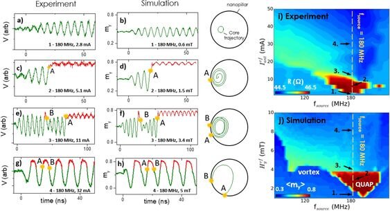
  • Spin dynamics and Spin Transfer Torque Nano-Oscillators.

  • Magnetic Annealing System (MATr 2000)

    The MATR is a system used for annealing at elevated temperatures (up to 400 °C) in the presence of intense magnetic fields (up to 2 Tesla). Such magnetic fields are generated by a superconducting magnet module created by running current through windings of this material. The system can handle multiple wafers of 200mm and 150mm in diameter, in parallel or perpendicular position with respect to the magnetic field. There is also a 1×1 inch sample holder available.

    UHV multi-target confocal sputtering tool (Kenosistec)

    A multi-target UHV sputtering system consisting of a deposition chamber with 11 2” diameter magnetrons in confocal geometry for the co-deposition of materials, optimised for wafers of up to 200mm in diameter.

    Ion Milling (Nordiko)

    A broad ion beam milling system for 200mm wafers, designed to provide a very good within-wafer uniformity at slow etch rates to indiscriminately remove thin layers of material, with effective sample cooling. It is equipped with end-point detection using secondary ion mass spectroscopy (SIMS) for very precise milling.

    TiW, AlSiCu, and Al2O3 Sputtering System (Timaris FTM)

    The Four-Target-Module (FTM) physical vapour deposition cluster tool is specially designed for the deposition of high–quality metallic, conductive and insulating films. The system is a UHV single wafer cluster tool and consists of one transport module, one multi-target PVD module with up to four DC/RF cathodes (three targets are installed in this machine AlSiCu, TiW and Al2O3) and one soft etch/oxidation module. It is capable of depositing different magnetic and non–magnetic layers on wafers with diameters up to 200mm by DC/RF Magnetron Sputtering, with good uniformity for the deposited films. The FTM incorporates Linear Dynamic Deposition (LDD) technology in combination with up to four sputter targets in one vacuum chamber. The LDD technology enables the capability to deposit wedge films with a different film thickness across the wafer and to deposit alloy films with adjustable concentration gradients across one wafer.

    Multi-target Sputtering Tool (Timaris MTM)

    The Multi-Target Module (MTM) physical vapour deposition cluster tool is specially designed for the deposition of ultra–thin films, magnetic films, high–quality metallic, conductive and insulating films and multiple film stack deposition comprising these materials without the need to break ultra-high vacuum. The system is a UHV single wafer cluster tool and consists of one transport module, one multi-target PVD module with 10 DC/RF cathodes and one soft etch/oxidation module. It is capable of depositing different magnetic and non–magnetic layers on wafers with diameters up to 200mm by DC/RF Magnetron Sputtering (or Ion Beam Sputtering), with good uniformity for the deposited stacks.
    Additional features such as wafer heating for hot substrate deposition or a collinear Aligning Magnetic Field (AMF) are available. The AMF can be activated to align the magnetic easy axis during the deposition of ferromagnetic films.
    The Linear Dynamic Deposition (LDD) technology enables the capability to deposit wedge films with different film thicknesses across the wafer and to deposit alloy films with adjustable concentration gradients across one wafer. Both features allow a very cost-effective development of film stacks and accelerate device development.

  • Current in-plane tester (CIPT)

    To verify the transport properties of MTJs before nanofabrication a  CIPT is used to perform TMR and RA measurements of bulk MTJ stacks. This is a very useful tool since it allows us to retrieve fundamental information of the MTJ stack prior to fabrication. To perform these measurements, the system contacts 12 cantilever electrodes with a variable spacing, down to 750 nm. It performs electrical measurements (current and voltage) through the different cantilevers with different spacing between them. This allows to determine the RA and TMR. The CIPT can determine RA values down to 0.1 Wμm² and measure the TMR with both in-plane and perpendicular anisotropy with in-plane fields up to 2500 Oe and perpendicular fields up to 1400 Oe.

    Vibrating Sample Magnetometer (VSM)

    The VSM allows the measurement of the magnetic moment as a function of the applied magnetic field of unpatterned samples. Thus, it allows us to measure and optimize the magnetic stack growth and magnetic annealings. The system can measure magnetic signals down to 5×10^-7 emu and very low coercivities (10 mOe; field resolution) and can apply fields up to 2 T. It allows fast and accurate measurements of the magnetic moment, not only as a function of the applied magnetic field but also with temperature (which can be swept from 83 to 570 K). Angular and time dependencies of the magnetization can be measured as well.

    Automatic Transport Measurement Setup (CIPT)

    Once the MTJ fabrication process is complete, this setup does a full characterisation of thousands of MTJ devices on the full wafer. A system with 40 tips, it can characterise 10 MTJs in a 4-contact scheme per landing site. Statistically meaningful data regarding the device TMR, RA, the shape of the transfer curves, and corresponding deviations arising from the nanofabrication process are obtained. Furthermore, the software allows the collection of different figures of merit (TMR, RA, coercive field, the linear range of the curve, etc) and organises them for different parameters (die number, pillar sizes, TMR and RA range, etc).

    RF Prober for in-plane magnetic fields

    Electrical contact to characterise RF devices was performed using special Cascade Microtech’s probes. These probes allow high-accuracy RF measurements with low contact resistance. It consists of an optical microscope in conjugation with holders that allow high-accuracy movements (both for the sample and the tips), used to connect the contacts to the device. The RF measurements can be performed while injecting a DC current in the MTJ.

    Synchronization and spin diode torque studies can also be performed since an RF signal can be provided to the MTJ and the generated DC voltage measured. The signal is then transported through coaxial cables to a 3 Hz – 44 GHz spectrum analyser where the emission spectrum can be acquired. Power suppliers are used to provide current both to the MTJ and the magnet.

    Automated control of the complete system can be performed to make sequences with different values of current and magnetic field. An amplifier is usually used to increase the measured signal, although its use was not necessary in the cases of MTJs with high output power. A bias tee is used to separate the DC and RF electrical components (being the last one sent to the spectrum analyser). The magnetic field was applied using a small magnet. The orientation of the magnet could be manually changed but it was limited to relatively small magnetic fields (up to 200 Oe) in the in-plane direction.

    RF Prober for out-of-plane magnetic fields

    Similar to the IP measurement setup, this is an RF measurement setup with power supplies and spectrum analyzer, but for out-of-plane magnetic fields. Magnetic fields up to 1.6 T can be applied. The magnetic field can be rotated between in-plane and out-of-plane directions with a highly precise stepper motor. The applied magnetic field value can be measured directly using a gaussmeter. The setup requires the positioning of the tips with the aid of an optical microscope. After the tips are properly connected to the contacts the microscope is easily displaced and the magnet is positioned in the sample position.

Projects

NIMFEIA

Nonlinear Magnons for Reservoir Computing in Reciprocal Space

REMAP

REusable MAsk Patterning

ATE

ATE - Aliança para a Transição Energética

BE.Neutral

BE.Neutral - Agenda de Mobilidade para a neutralidade carbónica nas cidades

GreenAuto

Green Innovation for the Automotive Industry

SWAN-on-chip

Low power spintronics wireless autonomous node (SWAN) integrated circuits developed via spintronics technology accelerator platform

RadioSpin

DEEP OSCILLATORY NEURAL NETWORKS COMPUTING AND LEARNING THROUGH THE DYNAMICS OF RF NEURONS INTERCONNECTED BY RF SPINTRONIC SYNAPSES

SpinAge

Weighted Spintronic-Nano-Oscillator-based Neuromorphic Computing System Assisted by laser for Cognitive Computing

PRODUTECH 4 S&C

PRODUTECH SUSTENTÁVEL & CIRCULAR - Soluções inovadoras, sustentáveis e circulares com impacto na fileira das tecnologias de produção

(LINK4S)ustainability

(LINK4S)ustainability – A new generation connectivity system for creation and integration of networks of objects for new sustainability paradigms

NeWeSt

New generation of cyberphysical Weighing Systems / Nova geração de Sistemas de Pesagem ciber-físicos

SPINAR

Spin-based hardware artificial neural network for embedded radio-frequency signal processing

INFANTE

Satélite para aplicações marítimas e comunicações a partir de constelações

Micro&NanoFabs@PT

Network of Micro and Nano Fabrication Research Facilities in Portugal

MAGLINE

Development and industrial validation of TMR sensors fabrication process

MOSAIC

MicrOwave Spintronics as an AlternatIve Path to Components and Systems for Telecommunications, Storage and Security Applications

Publications